
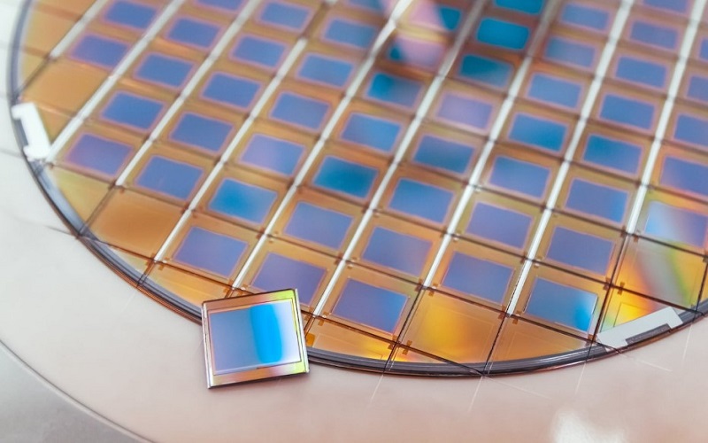
Wafer dicing is a critical step in the semiconductor manufacturing process, where a semiconductor wafer is divided into individual semiconductor chips, often referred to as die. This process is essential because it transforms a single large wafer containing multiple integrated circuits into separate chips that can be packaged and used in various electronic devices.
The wafer dicing process typically involves the following steps:
-
Wafer Inspection: Before dicing, the semiconductor wafer undergoes inspection to detect any defects or anomalies. Defective or damaged areas are marked for exclusion, ensuring that only good die are diced.
-
Alignment: The wafer is aligned properly in a dicing machine, ensuring that the dice will be cut precisely according to the design specifications. This step is crucial to maintain the integrity of the individual chips.
-
Dicing: Dicing is the actual cutting of the wafer into individual chips. This is typically done using specialized equipment, such as a dicing saw or laser dicing system. The choice of dicing method depends on the material properties of the wafer and the desired precision.
-
Mechanical Dicing (Sawing): In this method, a high-speed rotating blade (dicing saw) with abrasive particles cuts through the wafer. The saw creates a channel between the dice, and the wafer is gradually moved to separate the individual chips.
-
Laser Dicing: Laser dicing uses a high-energy laser beam to ablate and separate the material along the scribe lines, creating the gaps between dice. This method is often used for delicate or brittle materials.
-
-
Inspection and Quality Control: After dicing, another inspection step may be performed to ensure that each die is free from defects and that the dimensions and positioning meet the specifications. Any chips with defects or inaccuracies are typically marked or removed.
-
Die Sorting: The individual chips are sorted based on their characteristics, such as performance and quality. This step is important for matching chips that will be packaged together in the same device.
-
Cleaning: The diced chips are cleaned to remove any debris, particles, or residues left from the dicing process.
-
Packaging: Once the chips are diced, sorted, and cleaned, they are typically placed into packages. These packages provide electrical connections and protection for the semiconductor chip. Common packaging methods include chip-on-chip, chip-on-board, and various types of surface-mount packages.
-
Testing: The packaged chips undergo electrical testing to ensure that they function correctly. This testing may include functionality tests, parametric tests, and other quality control measures.
-
Final Inspection: The final packaged devices are inspected to ensure they meet the required specifications and quality standards.
-
Shipping: After passing all inspections and tests, the packaged chips are ready for distribution to manufacturers who will use them in various electronic devices.
The wafer dicing process is a crucial step in semiconductor manufacturing because it enables the production of individual chips from a single wafer, making them ready for use in a wide range of electronic applications, from microprocessors and memory chips to sensors and integrated circuits.